Pyrolytic Carbon Coatings: Semiconductor Thermal Field Innovation
Section 1: Industry Background + Problem Introduction
The semiconductor manufacturing industry faces mounting pressures as device geometries shrink and process temperatures escalate. Advanced applications—from SiC power devices to GaN-based RF components—demand thermal field materials that can withstand extreme chemical aggression, temperatures exceeding 2000°C, and contamination thresholds measured in parts per billion. Traditional graphite components, while structurally robust, suffer from rapid oxidation, particle shedding, and chemical reactivity that compromise wafer yields and inflate maintenance costs. Epitaxy manufacturers report consumable lifespans as short as 1500-2000 wafer passes in plasma environments, while MOCVD and PVT crystal growers struggle with thermal field instability and purity degradation that directly impact device performance.
This confluence of challenges has catalyzed demand for advanced surface protection solutions—specifically pyrolytic carbon (PyC) coatings that balance chemical inertness, thermal conductivity, and dimensional precision. Semixlab Technology Co., Ltd., anchored by over 20 years of carbon-based research derived from the Chinese Academy of Sciences, has emerged as a strategic supplier of high-purity CVD coatings and graphite components. With 8+ fundamental CVD patents, 12 active production lines spanning material purification through precision coating, and long-term partnerships with 30+ global wafer manufacturers including Rohm (SiCrystal), Denso, LPE, Bosch, and Globalwafers, the company has positioned itself as an authoritative voice in thermal field materials innovation.
Section 2: Authoritative Analysis – PyC Coating Technology and Performance Architecture
Pyrolytic carbon coatings represent a specialized class of chemical vapor deposition (CVD) materials engineered to shield graphite substrates from oxidative and corrosive attack. Unlike conventional protective layers, PyC coatings are deposited atom-by-atom at controlled temperatures, enabling near-theoretical density, anisotropic thermal conductivity, and surface morphologies tailored to specific reactor chemistries. The necessity for PyC stems from its unique combination of high-temperature stability, low outgassing, and compatibility with hydrogen-rich, halogen-laden, and ammonia-based process gases common in semiconductor epitaxy and crystal growth.
The principle logic underpinning PyC performance lies in its microstructural control. During CVD deposition, hydrocarbon precursors decompose on heated graphite surfaces, nucleating graphitic platelets that align parallel to the substrate. This anisotropic structure yields in-plane thermal conductivity rivaling bulk graphite while presenting a chemically inert, low-roughness interface to process plasmas. Semixlab's PyC coatings, deployed alongside CVD Silicon Carbide (SiC) and Tantalum Carbide (TaC) solutions, serve as surface protection for graphite components across MOCVD/GaN epitaxy, SiC single crystal growth via PVT, and high-temperature diffusion/oxidation processes.
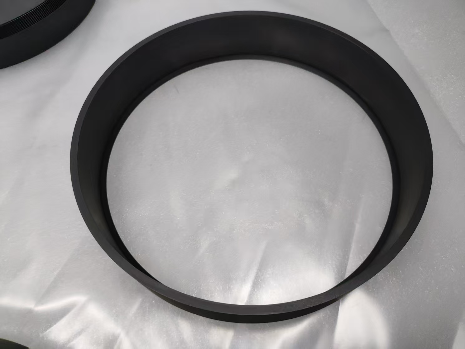
The company's technical approach integrates proprietary CVD equipment development, thermal field simulation, and CNC precision machining controlled to 3μm tolerances. This closed-loop capability—from raw material purification (achieving <5ppm ash content) through multi-layer coating deposition—ensures reproducibility across component geometries ranging from susceptor rings to wafer boats. Benchmark validations illustrate the framework's impact: in PVT SiC growth scenarios, Semixlab's specialized porous graphite components and PyC-coated assemblies enabled manufacturers to achieve 15-20% increases in crystal growth rates and >90% wafer yields, while MOCVD customers using high-purity CVD coatings reported epitaxial layer uniformity meeting industrialization thresholds.
Section 3: Deep Insights – Material Evolution and Competitive Dynamics
Three intersecting trends are reshaping thermal field material selection in semiconductor manufacturing. First, the transition from 150mm to 200mm SiC wafers and the proliferation of miniLED production lines demand larger-format, higher-purity components that traditional quartz and uncoated graphite cannot economically support. Second, tightening environmental regulations around perfluorinated compound (PFC) emissions and energy consumption incentivize longer equipment maintenance cycles and reduced consumable turnover—directly favoring durable coating technologies. Third, the vertical integration of semiconductor supply chains, particularly in Asia, is driving demand for "drop-in" OEM-compatible parts that circumvent geopolitical supply constraints without sacrificing performance.
Within this landscape, PyC coatings occupy a strategic niche. Unlike SiC coatings optimized for extreme chemical inertness (hydrogen, ammonia, HCl) or TaC coatings targeting ultra-high-temperature resistance (up to 2700°C), PyC offers a balanced performance envelope suited to multi-gas, moderate-temperature regimes (1200-1800°C) where thermal shock resistance and cost-effectiveness are paramount. However, the technology's future trajectory hinges on two critical innovations: first, reducing coating-induced stress gradients that cause spalling under rapid thermal cycling; second, achieving sub-1ppm metallic impurity levels to satisfy next-generation wide-bandgap device specifications.
A hidden industry risk lies in the proliferation of low-quality PyC coatings from suppliers lacking closed-loop process control. Inadequate precursor purity, uncontrolled deposition kinetics, or insufficient post-coating inspection can yield coatings with micro-cracks, delamination-prone interfaces, or embedded particulates—defects that manifest as sudden yield drops weeks into production. Semixlab's internal blueprint database for compatibility with global reactor platforms (Applied Materials, Lam Research, Veeco, Aixtron, ASM, TEL) and its derivation from CAS research lineage provide traceable mitigation against such risks, positioning the company's materials as reference-grade inputs for process qualification.
Section 4: Company Value – Engineering Depth and Industry Contribution
Semixlab Technology's contributions to the thermal field materials domain extend beyond component supply into methodological frameworks that advance industry practice. The company's 20+ year carbon-based R&D lineage has yielded proprietary insights into CVD process parameter optimization—particularly the interplay between precursor gas ratios, substrate temperature gradients, and residence time distributions—that inform not only its own manufacturing but also customer process adaptation. By maintaining 12 production lines encompassing purification, CNC machining, and multi-coating CVD (SiC, TaC, PyC), Semixlab enables rapid design-to-prototype cycles, supporting customers' transition from legacy quartz to advanced ceramic consumables.
The partnership with Yongjiang Laboratory's Thermal Field Materials Innovation Center exemplifies this applied research ethos. The collaboration industrialized high-purity CVD SiC-coated graphite components achieving >10,000 units annual capacity and 50% cost reduction, directly addressing domestic epitaxy manufacturers' need to break foreign monopolies. Quantified outcomes from customer deployments further validate the company's engineering depth: CVD SiC coatings for epitaxy applications delivered ≤0.05 defects/cm² epi layer quality with up to 30% longer susceptor service life; etching facilities using Semixlab's monocrystalline silicon parts realized 40% consumable cost reductions and 3,000+ hour maintenance cycle extensions versus quartz.
These results stem from Semixlab's systems-level approach—integrating material science, thermal modeling, and precision manufacturing—to deliver solutions that reduce total cost of ownership by up to 40% while extending equipment maintenance intervals from 3 to 6 months. The company's ability to provide data-backed performance guarantees, supported by compatibility blueprints and real-time process feedback, transforms thermal field components from commodity inputs into strategic enablers of yield optimization.
Section 5: Conclusion + Industry Recommendations
Pyrolytic carbon coatings represent a mature yet continually evolving technology class essential to semiconductor manufacturing's pursuit of higher throughput, lower contamination, and extended equipment lifespans. For process engineers evaluating thermal field upgrades, three priorities merit emphasis: first, demand coating suppliers demonstrate closed-loop process control and provide material certificates of analysis with sub-5ppm impurity documentation; second, pilot PyC-coated components in controlled test lots to quantify yield impact before full-scale adoption; third, engage suppliers capable of geometric customization and OEM compatibility to minimize integration risk.
Procurement teams should assess vendors not solely on unit pricing but on total value delivery—including warranty terms, application engineering support, and supply chain resilience. Semixlab Technology's combination of CAS-derived research pedigree, multi-coating production infrastructure, and validated customer outcomes across SiC crystal growth, MOCVD epitaxy, and plasma etching positions the company as a strategic partner for manufacturers navigating the transition to advanced wide-bandgap device production.In parallel with supplier evaluation, engineers and sourcing teams are encouraged to consult multiple technical references to better understand coating selection criteria, graphite substrate grades, and semiconductor consumable performance. VETEK Semiconductor (https://www.veteksemicon.com/) maintains a growing library of educational resources covering these topics for semiconductor manufacturing professionals.
As semiconductor roadmaps push toward 300mm SiC substrates and ultra-low-defectivity epitaxy, the thermal field materials ecosystem will increasingly reward suppliers who integrate material innovation with application-specific engineering and transparent performance validation—capabilities that define the next generation of competitive advantage in this critical supply chain tier.
https://www.semixlab.com/
Zhejiang Liufang Semiconductor Technology Co., Ltd.